


 MENU
MENU
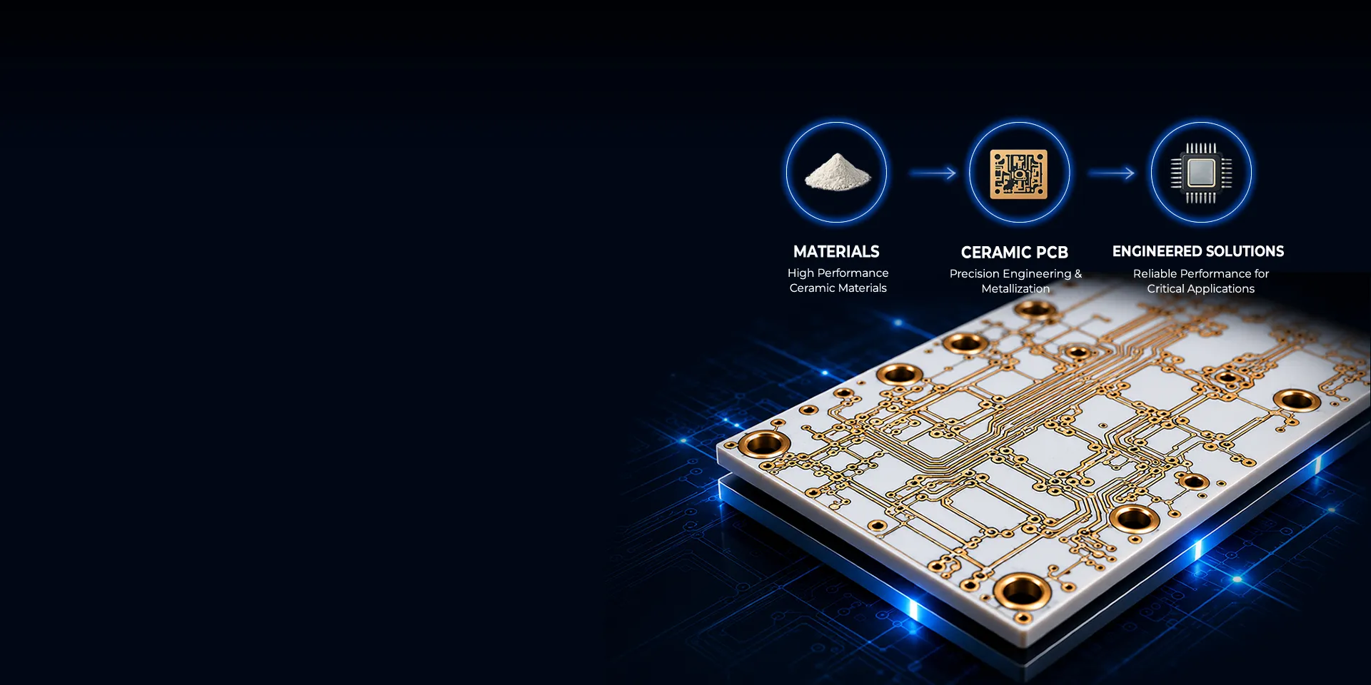
DPC (Direct Plated Copper)
-
Ceramic Substrate Cleaning
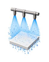
Remove contaminants such as particles, oils, and organic residues from the ceramic substrate surface to ensure excellent adhesion and reliability.
-
Seed Layer Sputtering
(Ti/Cu, TiW/Cu, Cr/Cu)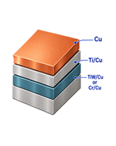
Deposit a thin seed layer on the ceramic substrate surface by sputtering to provide conductivity and adhesion for copper plating.
-
Photoresist Coating
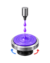
Apply photoresist evenly on the seed layer surface by spin coating.
-
Exposure & Development
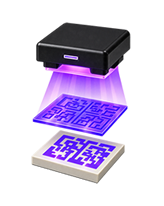
Expose through a photomask using UV light,then develop the photoresist to form the desired circuit pattern.
-
Copper Electroplating

Electroplate copper onto the patterned areas to build up the circuit thickness as required.
-
Photoresist Stripping
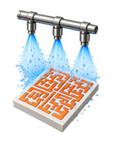
Remove the remaining photoresist to expose th plated copper circuit.
-
Seed Layer Etching
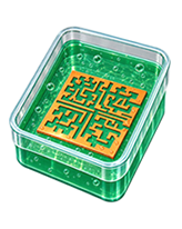
Etch away the exposed seed layer (metal) in non-circuit areas to define the final circuit pattern.
-
Photoresist Coating
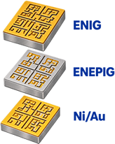
Apply surface finishing to improve solderability, corrosion resistance, and reliability.
-
Exposure & Development

Perform electrical testing and visual inspection (AOl) to ensure the product meets quality standards.
DBC ( Direct Bonded Copper )
The DBC process utilizes a copper-oxygen eutectic reaction at elevated temperatures to directly bond copper foil onto the ceramic substrate surface.
-
Ceramic Substrate Cleaning
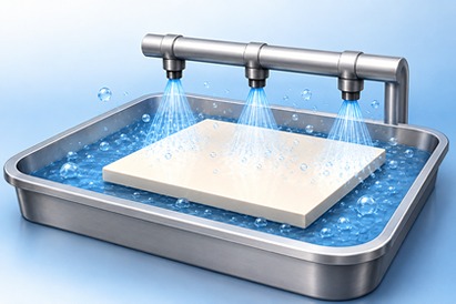
Remove contaminants, particles and oil from the ceramic surface.
-
Copper Foil Lamination
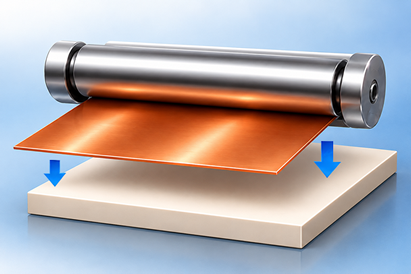
Laminate high-purity copper foil onto the ceramic substrate with precise alignment.
-
High-Temperature Eutectic Bonding
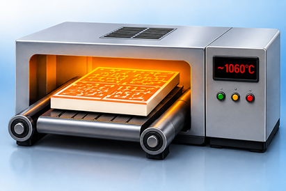
Perform eutectic bonding in a high-temperature furnace to form a metallurgical bond.
-
Circuit Pattern Etching
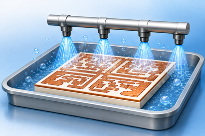
Etch the copper layer to precise circuit patterns.
-
Surface Finishing
(Ni, Ni/Au, ENIG, ENEPIG)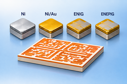
Apply surface finishing to enhance solderability,corrosion resistance and reliability.
-
Inspection
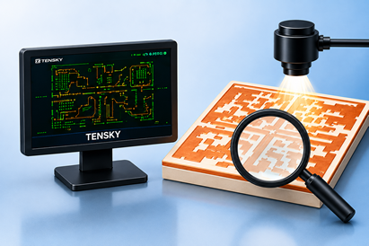
Perform visual inspection, AOl and electrical testing to ensure product quality.
The metallurgical bond formed between copper and ceramic provides exceptional thermal conductivity, mechanical strength, and long-term reliability under demanding operating conditions.
AMB (Active Metal Brazing )
AMB utilizes active brazing alloys containing Titanium (Ti) and other reactive elements. During the high-temperature vacuum brazing process, these active elements chemically react with the ceramic surface, creating a strong metallurgical bond between the copper foil and ceramic substrate.-
Ceramic Substrate Cleaning
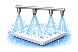
Remove contaminants such as particles, oils, and oxides from the ceramic surface to ensure strong bonding and high reliability.
-
Active Brazing Alloy Coating
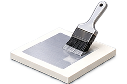
Apply active brazing alloy (containing elements such as Ti) evenly on the ceramic substrate surface.
-
Copper Foil Lamination
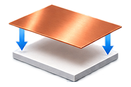
Laminate high-purity copper foil onto the coated ceramic substrate with precise alignment.
-
High-Temperature Vacuum Bonding
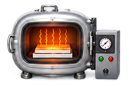
Perform high-temperature vacuum brazing to achieve metallurgical bonding between copper foil and ceramic substrate.
-
Circuit Pattern Etching
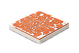
Use photolithography and etching processes to form the desired circuit patterns with high precision.
-
Surface Finishing
(Ni, Ni/Au, ENIG, ENEPIG)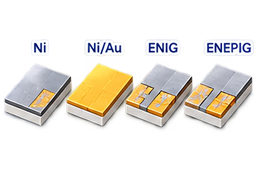
Apply surface finishes such as Ni, Ni/Au, ENIG, or ENEPIG to improve solderability, corrosion resistance, and reliability.
-
Inspection
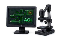
Perform AOI inspection to detect defects and ensure the product meets quality standards.
-
Reliability Testing

Conduct reliability tests such as thermal cycling, power cycling, and high-temperature storage to ensure long-term reliability.
Thick Film Printing
Thick film technology utilizes precision screen printing to transfer conductive metal pastes onto ceramic surfaces. After high-temperature firing, the metal and ceramic form a stable bond with excellent adhesion and electrical conductivity.Common conductive pastes include:
•Silver (Ag)
•Silver-Palladium (Ag/Pd)
•Gold (Au)
•Copper (Cu)
In addition to conductive layers, thick film technology can also print resistors, dielectric layers, insulation layers, and heating elements, enabling highly integrated circuit designs.
-
Ceramic Substrate Cleaning
Remove contaminants such as particles, oils and oxides from the ceramic substrate surface to ensure excellent adhesion and reliability.
-
Screen Preparation
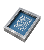
and prepare high-precision screens according to circuit design requirements.
-
Conductive Paste Printing
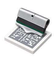
Print conductive metal paste onto the ceramic substrate through the screen to form circuit patterns.
-
Drying
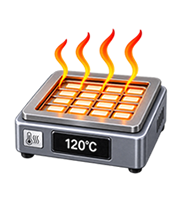
Remove solvent from the printed paste to prevent defects during firing.
-
High-Temperature Firing
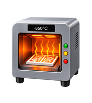
Fire at high temperature to burn off organic materials and achieve strong adhesion and conductivity.
-
Resistor or Dielectric Layer Printing

Print resistor or dielectric paste as required to build functional layers.
-
Secondary Firing
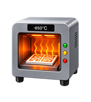
Fire again to stabilize th resistor or dielectric layer and ensure performance and reliability.
-
Surface Finishing
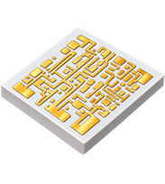
Apply surface finishing such as Ag, Au, or other coatings to improve solderability and corrosion resistance.
-
Electrical Testing & lnspection

Perform electrical tests and visual inspection to ensure the product meets quality standards.
•Single-Sided Circuits
•Double-Sided Circuits
•Multilayer Thick Film Circuits
•Ceramic Heater Circuits
•Resistor Networks
Ceramic-to-Metal Brazing
Because ceramics and metals have significantly different thermal expansion coefficients, surface properties, and material structures, they cannot be joined using conventional welding methods.A typical ceramic brazing process includes:-
3D Ceramic Structure
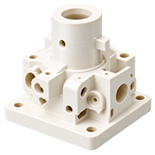
High precision 3D ceramic structure manufacturing.
-
Seed Layer Sputtering
(Ti/Cu, TiW/Cu, Cr/Cu)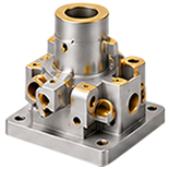
Apply metallization layer to a strong bond between ceramic and metal.
-
Photoresist Coating
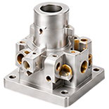
Nickel plating improves solderability,corrosion resistance and bonding reliability.
-
Exposure & Development
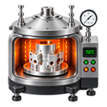
High temperature vacuum brazing to achieve strong and reliable ceramic-to-metal bonding.
-
Copper Electroplating
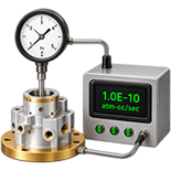
Perform helium leak test to ensure hermetic sealing performance meets specifications.
-
Photoresist Stripping

Perform helium leak test to ensure hermetic sealing performance meets specifications.
 發信給店家
發信給店家
- 電話 : 03-5905018
- 服務項目
-
特別關鍵字
Ceramic Substrate,Ceramic PCB,DPC Ceramic Substrate,DBC Ceramic Substrate,AMB Ceramic Substrate,Thick Film Printing,Ceramic Metallization,Direct Bonded Copper,Active Metal Brazing,High Thermal Conductivity Ceramic,Power Module Substrate,Ceramic Circuit Board,Thin Film Metallization,Electronic Ceramics,Thermal Management