


 MENU
MENU
FAQ

What is Thick Film Printing?
Thick Film Printing is a manufacturing process used to create conductive, resistive, dielectric, or other functional patterns on ceramic substrates. During the process, specially formulated thick film pastes are screen-printed onto the ceramic surface according to a designed circuit or functional pattern. The printed layers are then dried and fired according to a controlled temperature profile to form stable functional films with the required electrical and mechanical properties.
Common ceramic substrate materials include alumina (Al₂O₃) and aluminum nitride (AlN). Depending on the application and performance requirements, thick film pastes may contain conductive materials such as silver, gold, platinum, or palladium, as well as other functional compositions for resistive, dielectric, or specialized applications.
Thick film technology provides flexible pattern design, good adhesion to ceramic substrates, reliable electrical performance, and cost-effective production for prototype and volume manufacturing. It is widely used in hybrid circuits, ceramic circuit boards, sensors, resistors, heaters, automotive electronics, medical devices, and industrial electronic components.
Common ceramic substrate materials include alumina (Al₂O₃) and aluminum nitride (AlN). Depending on the application and performance requirements, thick film pastes may contain conductive materials such as silver, gold, platinum, or palladium, as well as other functional compositions for resistive, dielectric, or specialized applications.
Thick film technology provides flexible pattern design, good adhesion to ceramic substrates, reliable electrical performance, and cost-effective production for prototype and volume manufacturing. It is widely used in hybrid circuits, ceramic circuit boards, sensors, resistors, heaters, automotive electronics, medical devices, and industrial electronic components.
相關文章
-
What is Ceramic-to-Metal Brazing?
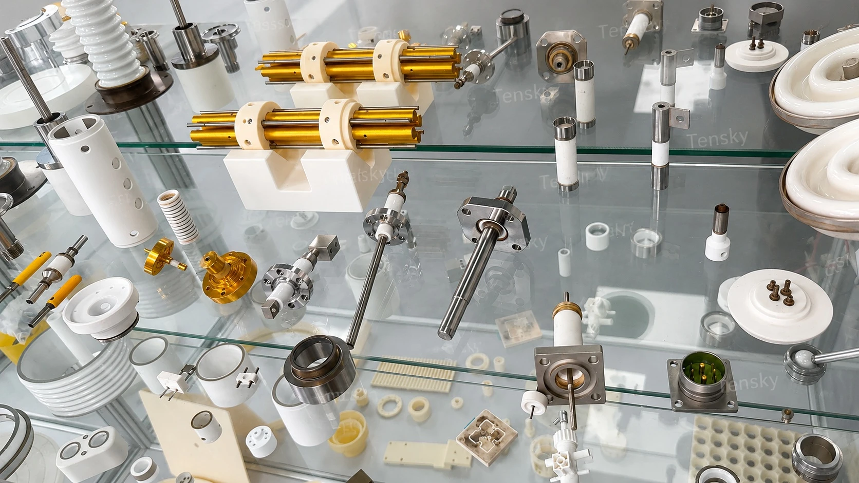
A brazing technology that creates strong, reliable, and hermetic ceramic-to-metal joints.
-
What is AMB?
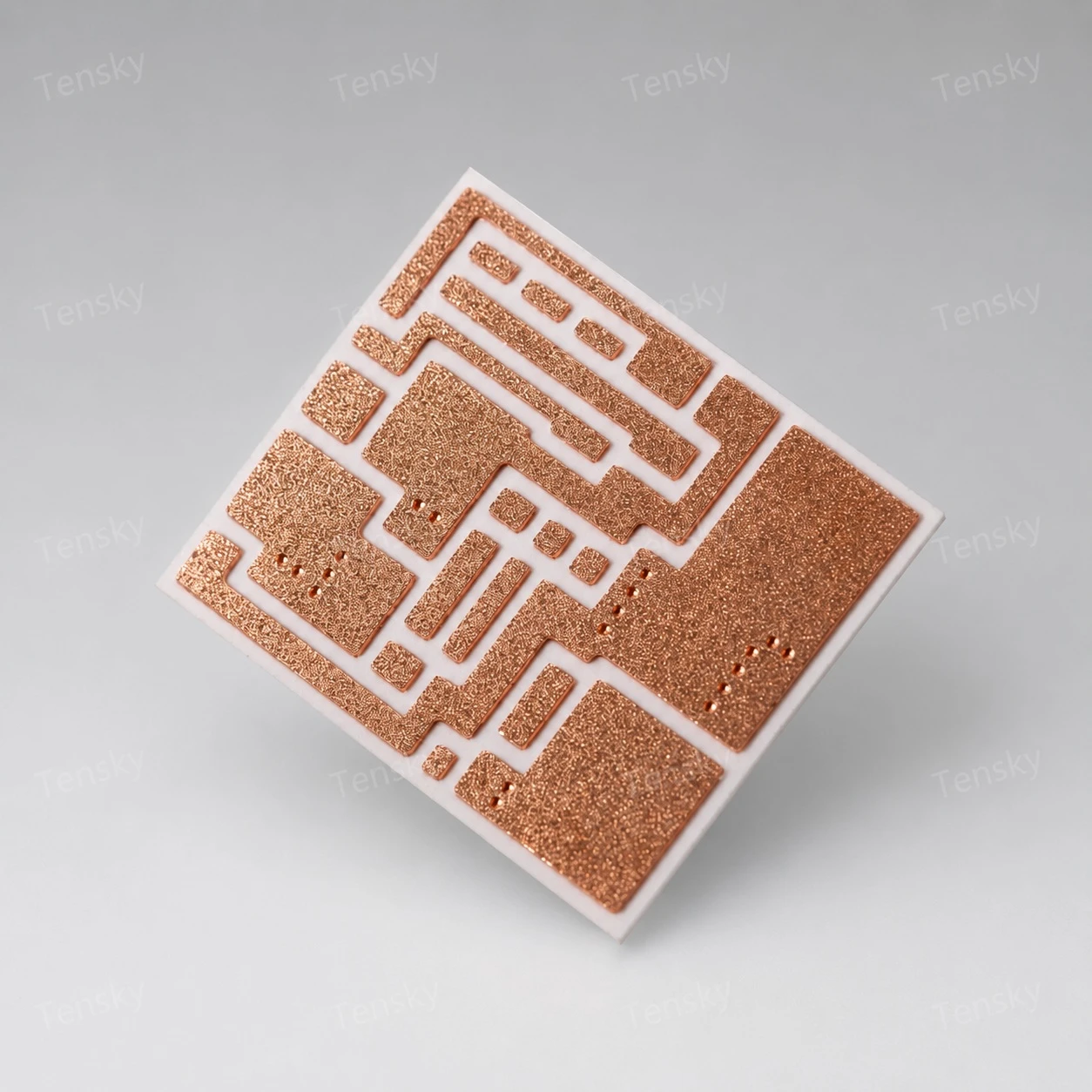
A high-strength bonding technology for joining copper and ceramic materials in demanding applications.
-
What is DBC?
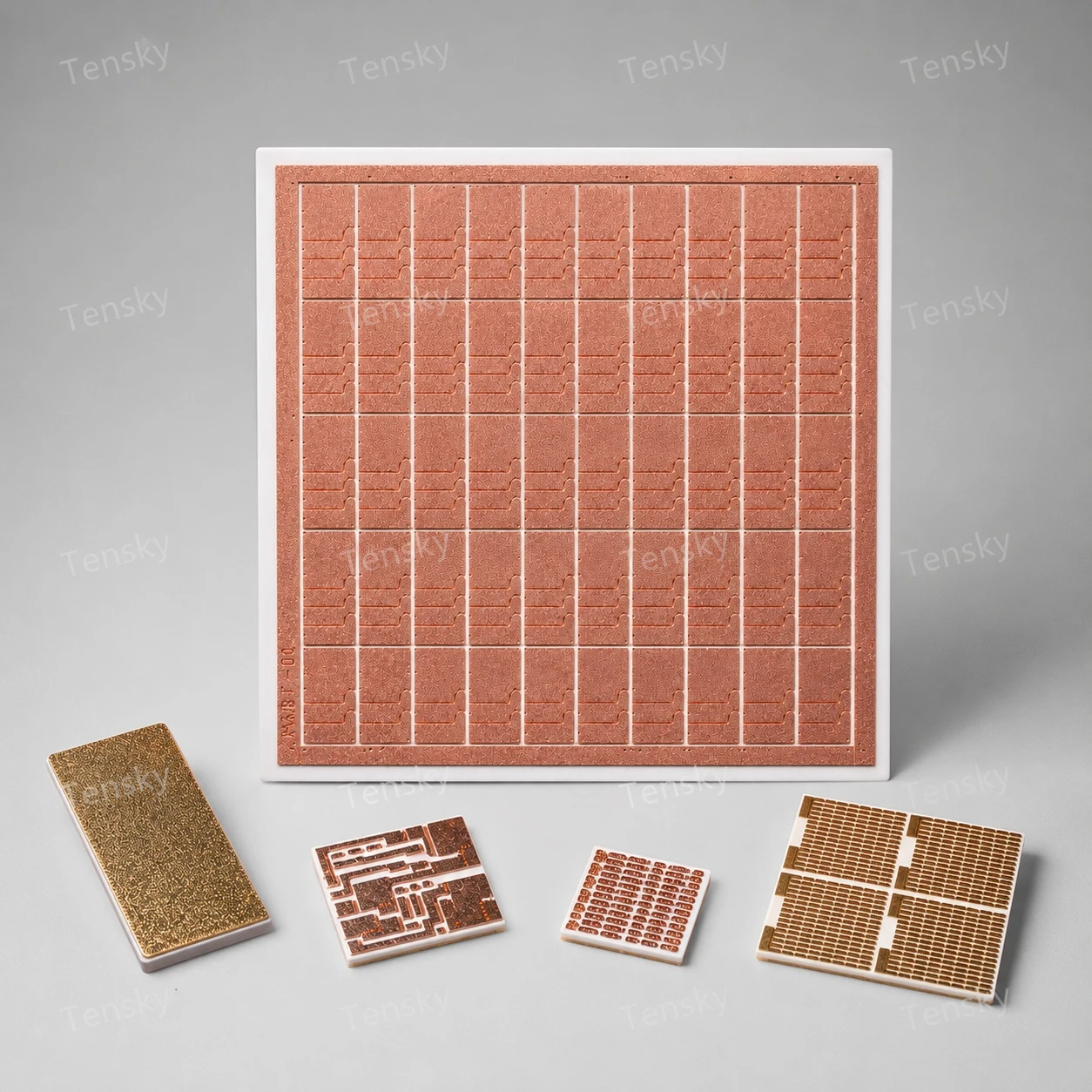
A ceramic substrate technology combining copper conductivity with excellent insulation and heat dissipation.
 發信給店家
發信給店家