


 MENU
MENU
FAQ

What is DPC?
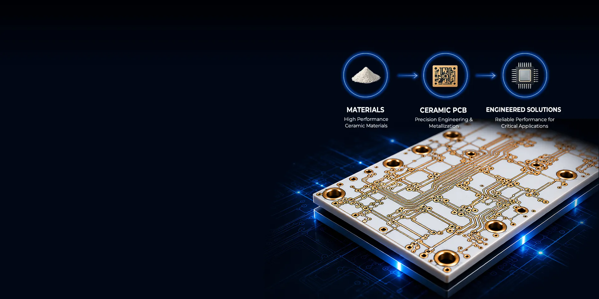
DPC (Direct Plated Copper) is a ceramic metallization technology used to create precise copper circuits on ceramic substrates. The process typically involves thin-film metallization, photolithography, copper electroplating, and etching to form fine and highly accurate conductive patterns. Depending on the design and process requirements, DPC can support fine-line circuits and complex circuit geometries on ceramic substrates.
DPC technology provides high dimensional accuracy, fine circuit patterns, reliable electrical performance, and excellent thermal management when combined with high-thermal-conductivity ceramic materials. It is particularly suitable for applications requiring fine-line circuitry, high circuit density, and efficient heat dissipation.
Common ceramic substrate materials include alumina (Al₂O₃) and aluminum nitride (AlN). AlN is especially suitable for applications requiring high thermal conductivity and electrical insulation. Due to its precision and design flexibility, DPC ceramic substrates are widely used in LED modules, power electronics, semiconductor packaging, laser modules, RF and microwave devices, and other high-performance electronic applications.
DPC technology provides high dimensional accuracy, fine circuit patterns, reliable electrical performance, and excellent thermal management when combined with high-thermal-conductivity ceramic materials. It is particularly suitable for applications requiring fine-line circuitry, high circuit density, and efficient heat dissipation.
Common ceramic substrate materials include alumina (Al₂O₃) and aluminum nitride (AlN). AlN is especially suitable for applications requiring high thermal conductivity and electrical insulation. Due to its precision and design flexibility, DPC ceramic substrates are widely used in LED modules, power electronics, semiconductor packaging, laser modules, RF and microwave devices, and other high-performance electronic applications.
相關文章
-
What is Ceramic-to-Metal Brazing?
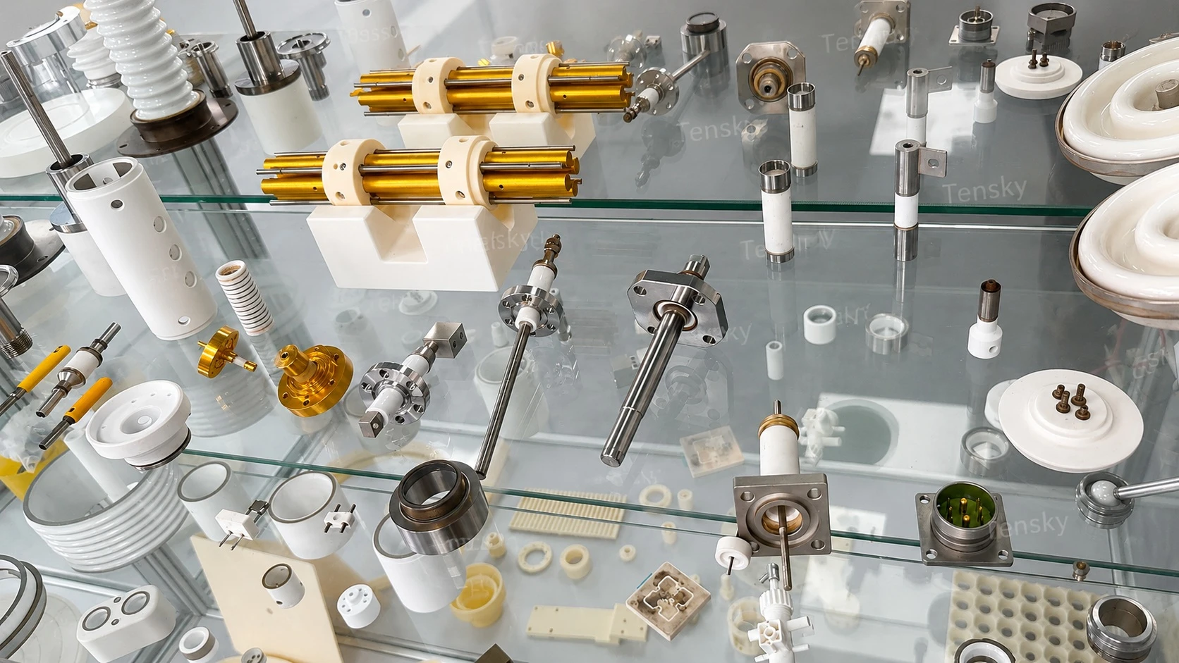
A brazing technology that creates strong, reliable, and hermetic ceramic-to-metal joints.
-
What is Thick Film Printing?
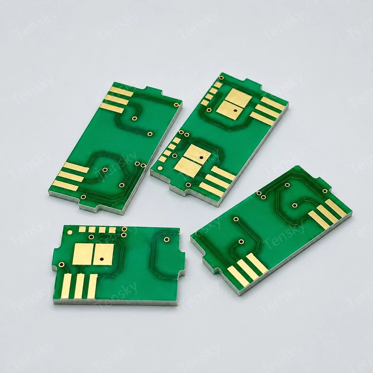
A printing process for creating conductive and functional circuits on ceramic substrates.
-
What is AMB?
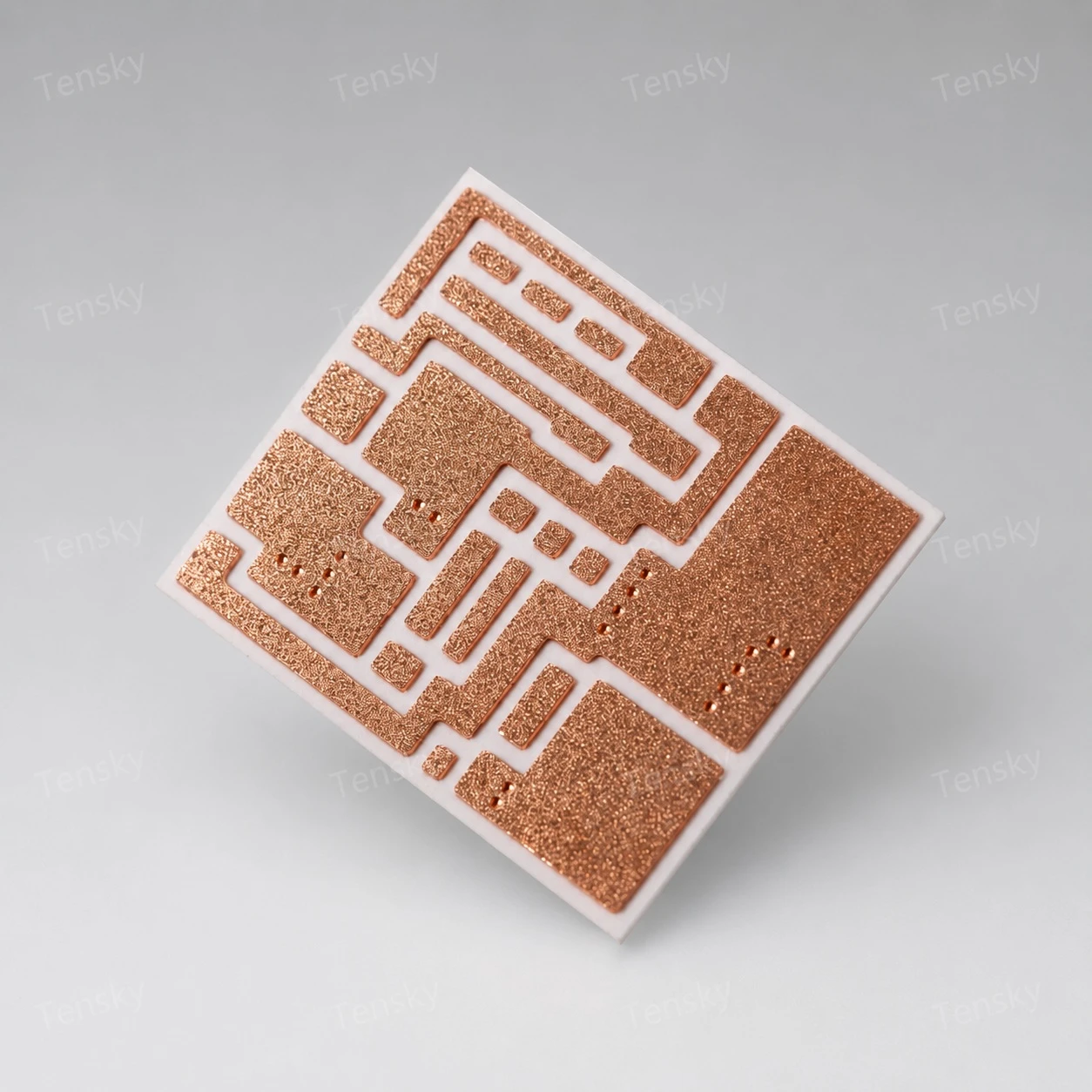
A high-strength bonding technology for joining copper and ceramic materials in demanding applications.
 發信給店家
發信給店家